


Advanced Solutions with GW PCB’s 12 Layer PCBs,12 layer pcb China Manufacturer
Free shipping on orders over $50!
- Satisfaction Guaranteed
- No Hassle Refunds
- Secure Payments
- Introduction to 12 Layer PCBs
- Importance and Applications
- High-Performance Features of GW PCB’s 12 Layer PCBs
- Quality and Reliability
- Diverse Industry Applications
- Communication, Aerospace, and More
- Customization and Flexibility
- Tailored Solutions for Unique Needs
- Advanced Manufacturing Capabilities
- State-of-the-Art Technology and Expertise
- Commitment to Sustainability and Compliance
- Environmental Responsibility and Industry Standards
- Why Choose GW PCB for Your 12 Layer PCB Needs
- Customer Focus and Global Reach
1. Introduction to 12 Layer PCBs
Importance and Applications
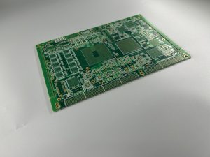
12 Layer PCBs: An Overview
The 12 layer PCB, a sophisticated type of printed circuit board, is renowned for its complexity and efficiency. These multi-layered boards are essential for advanced electronic applications due to their ability to support intricate circuits while maintaining a compact form factor.
Applications
They are pivotal in industries where high-speed signal transmission and extensive connectivity are crucial. The most common applications include data servers, GPS technology, satellite systems, and high-frequency applications in telecommunications and aerospace.
2. High-Performance Features of GW PCB’s 12 Layer PCBs
Quality and Reliability
Unmatched Quality Standards
GW PCB’s 12 layer PCBs stand out in the market for their exceptional quality. Each layer is crafted with precision, ensuring optimal electrical performance and reliability. The use of high-grade materials reduces the risk of issues like signal loss, ensuring stable operation in demanding environments.
Reliability in Complex Circuits
These PCBs undergo rigorous testing to meet stringent quality standards. The multilayer design allows for efficient heat dissipation, reducing thermal stress and enhancing longevity. This makes them ideal for applications requiring long-term reliability, such as in medical devices or military equipment.
3. Diverse Industry Applications
Communication, Aerospace, and More
Broad Industry Reach
The versatility of GW PCB’s 12 layer PCBs enables their use across various industries. In the communication sector, they support high-speed data transmission, essential for modern telecommunication networks. In aerospace, they are used in critical systems of aircraft and satellites, where reliability is paramount.
Emerging Technologies
These PCBs are also significant in emerging technologies like IoT and AI, where complex circuitry and high-speed data processing are required. Their robust design makes them suitable for automotive applications, particularly in electric and autonomous vehicles.
4. Customization and Flexibility
Tailored Solutions for Unique Needs
Meeting Specific Requirements
GW PCB understands that different applications have unique requirements. Therefore, the company offers customized solutions for its 12 layer PCBs. Customers can specify parameters like board thickness, material type, and surface finish to meet their specific needs.
Design Support and Flexibility
The company’s design team works closely with clients to ensure that the final product aligns with their specifications. This collaborative approach allows for flexibility in design and manufacturing, ensuring that the PCBs are optimized for their intended application.
5. Advanced Manufacturing Capabilities
State-of-the-Art Technology and Expertise
Leading-Edge Manufacturing Technology
GW PCB leverages the latest in manufacturing technology to produce its 12 layer PCBs. This includes advanced automation systems, high-resolution imaging techniques, and precision etching processes. These technologies ensure high accuracy and consistency in every PCB produced.
Expertise and Innovation
With a team of experienced engineers and technicians, GW PCB continuously innovates its manufacturing processes. This expertise not only enhances the quality of the PCBs but also allows for the efficient production of complex designs, meeting the high demands of various industries.
6. Commitment to Sustainability and Compliance
Environmental Responsibility and Industry Standards
Sustainable Practices
GW PCB is committed to sustainability, recognizing the importance of environmental responsibility in manufacturing. The company adopts eco-friendly processes and materials, minimizing waste and reducing the environmental impact.
Adherence to Compliance Standards
All 12 layer PCBs are manufactured in compliance with international standards such as ISO, UL, and RoHS. This commitment to compliance ensures that the products are not only high-quality but also meet the safety and regulatory requirements of different markets.
7. Why Choose GW PCB for Your 12 Layer PCB Needs
Customer Focus and Global Reach
Customer-Centric Approach
At GW PCB, the focus is always on the customer. The company prides itself on its ability to provide personalized service, technical support, and after-sales care. This customer-centric approach has earned GW PCB a reputation for reliability and trustworthiness in the industry.
Global Reach and Accessibility
With a global presence, GW PCB serves clients worldwide, ensuring timely delivery and accessibility. Whether it’s a small-scale project or a large-scale production, the company’s extensive network and logistic capabilities ensure that customer needs are met efficiently and effectively.